How Does a Photo Get Stored in Your Phone?
How Does a Phone Take a Photo? explained how photons striking the camera chip become electrons that can be counted. After you press the shutter, the photo has to be stored.
What gets stored is a string of 0s and 1s. Each 0 or 1 is a “bit,” the smallest unit of information; 8 bits make a “byte.” Photos vary in size; taking one of 3 MB (3 million bytes) as an estimate, that is bits. Turn the phone off, let the battery die, leave it for years, switch it back on, and they are all still there.
Where are they kept? Why doesn’t switching off the power wipe them?
Two common guesses
There are two common guesses:
- “Like tapes and hard disks, it’s recorded magnetically.” The spinning hard disk in a computer does work that way, magnetising tiny patches of a platter. But there is no spinning platter in a phone.
- “If it’s stored electrically, the power has to stay on.” A computer’s memory (RAM) does work that way, and forgets everything when the power goes off. Yet a phone that’s switched off still has its photos.
Phones use a third way: flash memory. It stores each bit as a small cluster of electrons, locked on an “island” inside the chip.
Where does a bit live?
A flash chip is packed with hundreds of billions of “memory cells.” Each cell is a tiny transistor:
- At the bottom is a block of silicon with two conducting regions, the source and the drain, like the inlet and outlet of a water pipe; electrons flowing from source to drain are an electric current.
- On top is the control gate, where voltage is applied, like a valve on the pipe that decides whether current flows.
- In between is an extra layer: an island, walled in by insulators above and below, built just for storing electrons.
Reading doesn’t mean taking the electrons off the island to look. Electrons are negatively charged and repel each other: electrons on the island push away the electrons at the silicon surface below. So with the same few volts on the control gate, an empty cell forms a channel and current flows, read as 1; a written cell can’t form one, no current flows, read as 0.
The insulator around the island is silicon dioxide, the main ingredient of optical-fibre glass. Even after years, the electrons on the island can’t get out and others can’t get in. In early flash the island was a small piece of conducting silicon; in the flash in today’s phones it is a layer of silicon nitride, with electrons stuck in its “traps.” The idea is the same.
But that raises a puzzle: if the insulator is so tight, how do electrons get onto the island when writing?
How electrons pass through walls: quantum tunnelling
First, how high is this wall? Energy is often measured in electronvolts: the energy an electron gains when accelerated through 1 volt is 1 electronvolt (eV). An electron in silicon must jump a step about 3.1 eV high to enter silicon dioxide: that is the height of the insulating “wall.” At room temperature an electron’s thermal energy is only about 0.025 eV, more than a hundred times less. Classically, it can only bounce back, like a ball thrown at a wall taller than it can jump.
Quantum mechanics says otherwise. An electron is also a wave, and a wave hitting a wall seeps in a little, fading fast inside it; if the wall is thin enough, a small part always comes out the other side. This is “quantum tunnelling.”
The fraction that gets through falls exponentially with the thickness of the wall. Estimating with the numbers for silicon dioxide: for a wall 1 nm thick, the chance of an electron getting through on one hit is about ; at 5 nm, about ; at 8 nm, about .
Tunnelling works both ways: electrons outside can tunnel in, and electrons on the island can tunnel out. But for an 8 nm wall, even if an electron on the island hits the wall about times a second, it would take about years on average to get out once, trillions of times the age of the universe. The wall is this thick precisely so that normally no electron gets through either way. But then electrons can’t get through when we want to write, either. The answer is a voltage.
A voltage makes the wall “thinner”
Put about 20 V on the control gate and a strong electric field appears in the insulator, roughly 1 V per nanometre. What the voltage does is tilt the whole energy “landscape” down towards the island: the closer to the island, the lower an electron’s energy.
Think of it as a piece of land: on the silicon side the ground is flat and the electron stands on it; the insulator is a plateau 3.1 eV high; the island is on the far side of the plateau. Applying the voltage is like tilting the land down towards the island: on the electron’s side the plateau is as high as before, but further in it keeps dropping, until at some point it is lower than where the electron stands. The wall itself hasn’t changed, but the part that rises above the electron is now only a thin slice at the front.
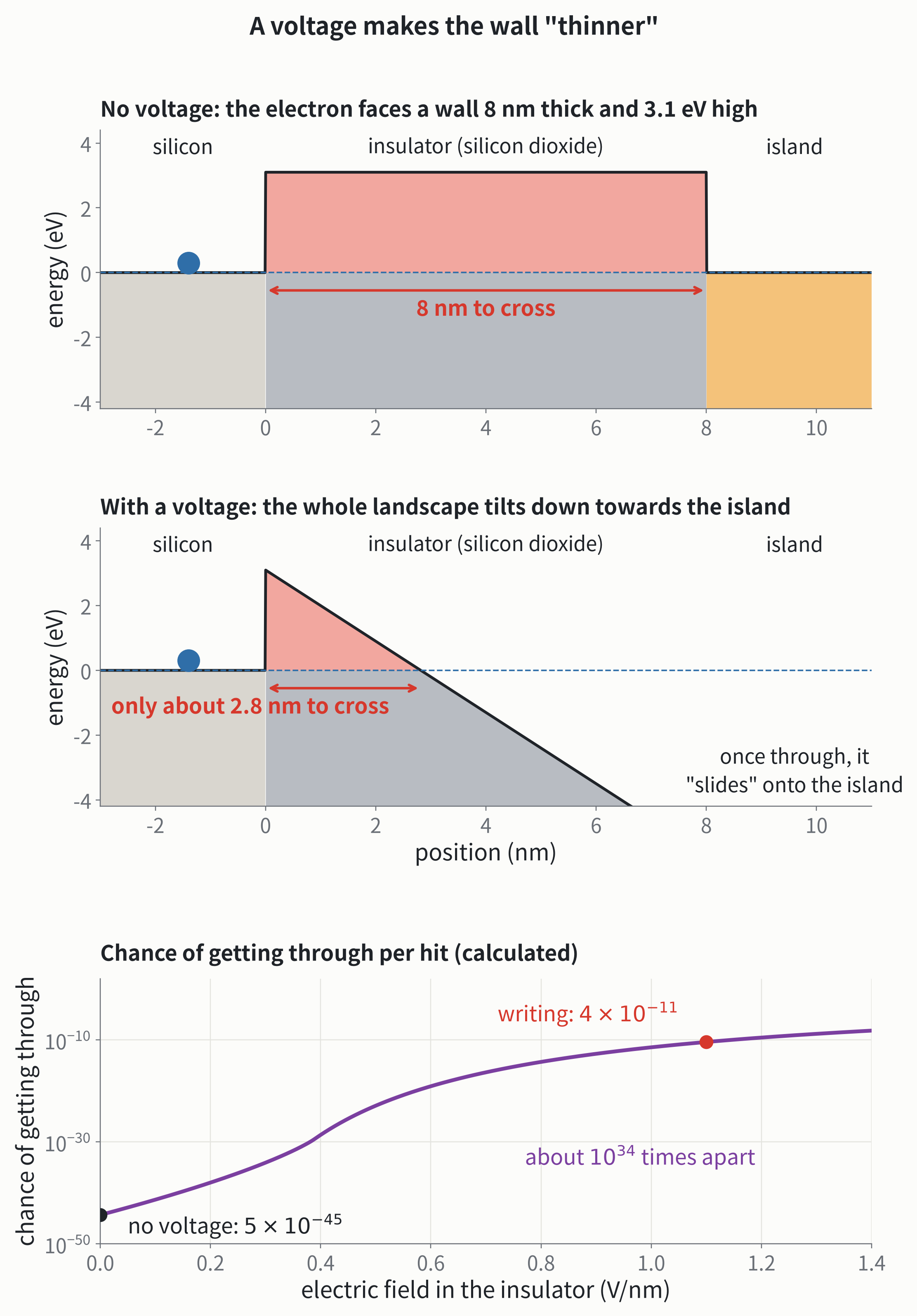
Switching the voltage on and off changes the chance of tunnelling by about times: that is the “switch” of flash memory. When writing, the wall only gets thinner for electrons moving with the field: electrons tunnel from the silicon onto the island, hundreds of them in less than a millisecond; when the voltage is removed, the wall is back as it was and the electrons are locked in. To erase, the voltage is applied the other way, the wall tilts the other way, and the electrons are pulled back into the silicon.
20 V, when a phone battery gives only about 4 V? The flash chip contains circuits called “charge pumps” that step a few volts up, stage by stage. Today’s flash still writes with 15 to 25 V, applied as a series of pulses rising a little at a time, so that each cell stops at exactly the right level.
Tunnelling through a barrier tilted by a strong field was worked out in 1928 by Ralph Fowler and Lothar Nordheim, and is called Fowler-Nordheim tunnelling. In 1957, Leo Esaki, working at Tokyo Tsushin Kogyo (later Sony), made the first semiconductor diode that worked by tunnelling, and won the 1973 Nobel Prize in Physics. The 2025 Nobel Prize in Physics went to John Clarke, Michel Devoret and John Martinis, who saw quantum tunnelling of a whole electric circuit on a chip; it is the basis of today’s superconducting quantum computers.
One cell, 4 bits
The earliest flash cells told apart only “electrons” and “no electrons,” storing 1 bit. Then engineers realised that a few more or fewer electrons make the channel harder or easier to form, which also reads differently, so why not use more levels? With 4 levels a cell stores 2 bits; 8 levels, 3 bits; 16 levels, 4 bits. The flash in today’s phones mostly stores 3 bits per cell, and some stores 4.
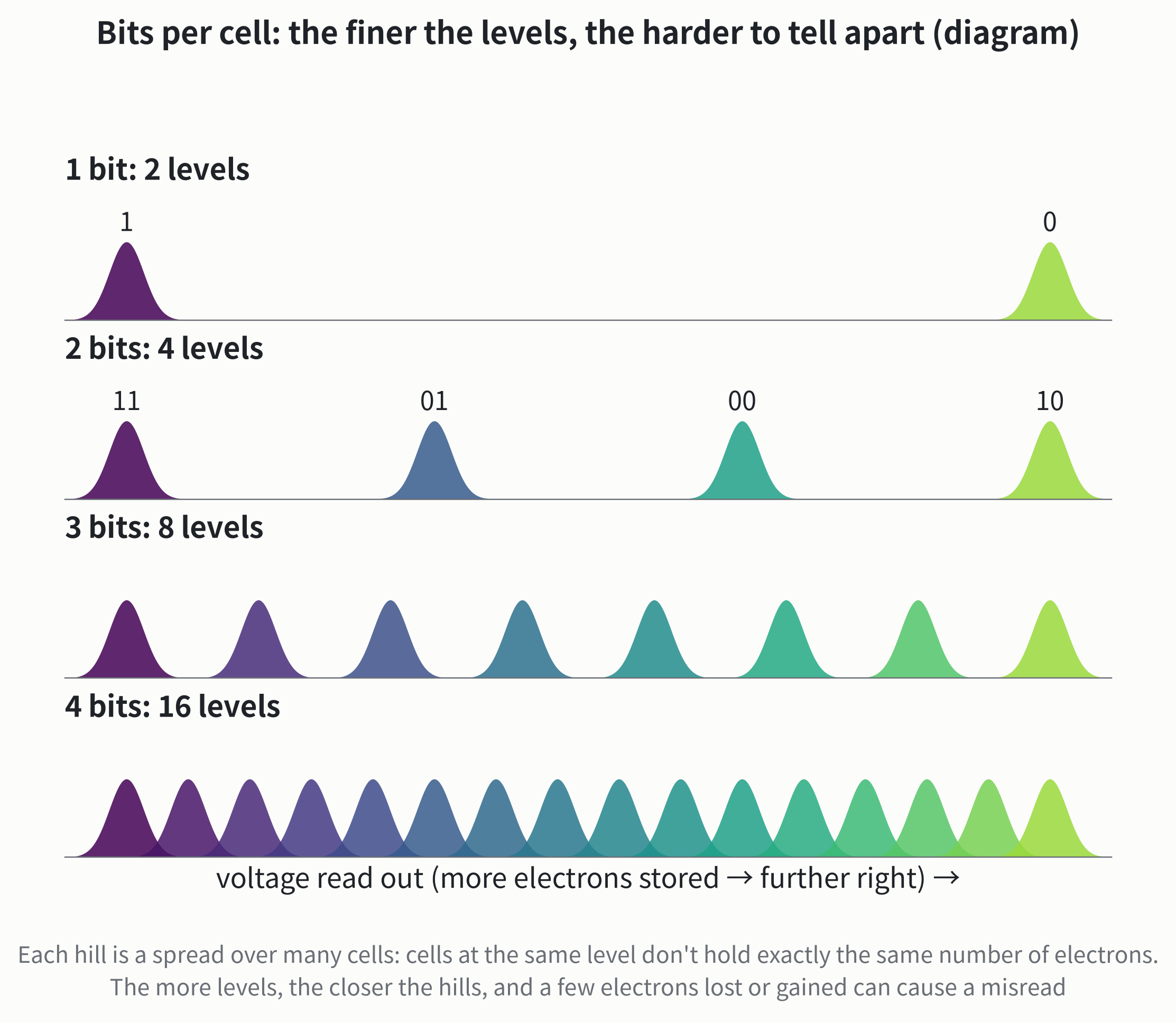
The price is that the levels get harder to tell apart. A cell holds only a few hundred electrons in all; split into 16 levels, neighbouring levels differ by a few tens of electrons, or even a dozen or so. Lose or gain a few electrons and a cell can be misread. So a phone’s flash chip also runs error-correcting codes that put misread bits right.
A phone’s flash chips hold more and more cells, too. Today’s flash stacks its cells layer upon layer, up to more than three hundred layers, like a building hundreds of storeys tall with every floor covered in cells. A 256 GB phone holds about bits; at 3 bits per cell, that is about 700 billion cells.
How many years does a phone’s flash last?
Each time an electron tunnels through the wall, it does a tiny bit of damage to the insulator, and sometimes an electron gets stuck inside the wall. After many writes and erases the wall leaks more and more, until it can no longer hold electrons in. How many times a cell can be rewritten depends on how many levels it uses: one storing 1 bit can be written about 100,000 times; one storing 3 bits, about one to a few thousand; one storing 4 bits, about a thousand.
That doesn’t sound like much, but a phone uses its cells “in turn,” so that no part wears out first. A rough estimate: 256 GB of flash, each cell written a thousand times, can take about 256 TB in all; the chip also has to rewrite some data internally, so call it 100 TB of real writing. Even writing 20 GB a day (plenty of photos and videos, app updates, caches from streaming), that lasts more than ten years, far longer than a phone.
In 2019, researchers at the University of North Carolina tested several phones and found that ordinary apps really don’t wear out the flash; but a malicious app writing nonstop could wear out an older 8 GB phone in a few days.
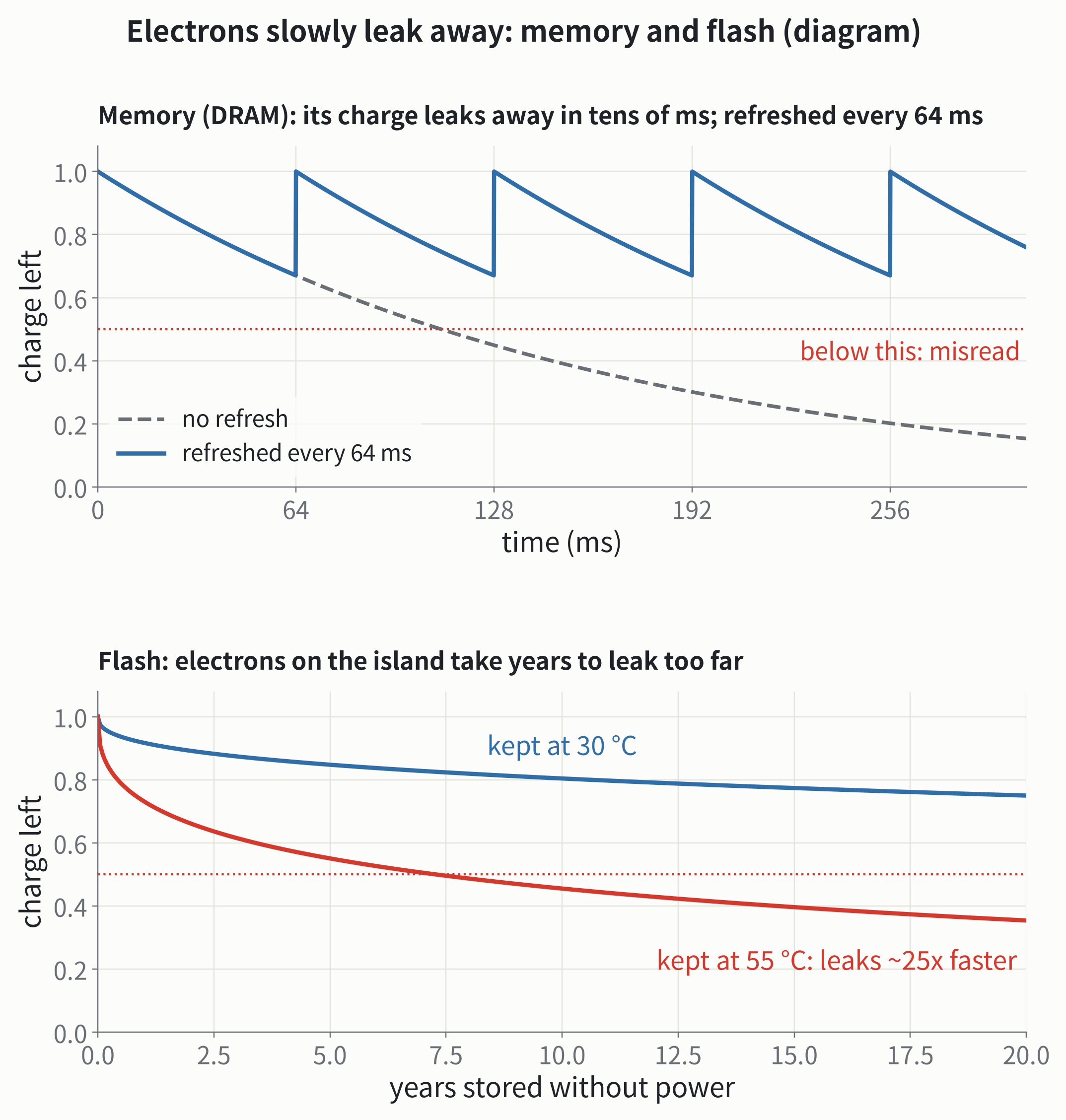
Even when nothing is written, electrons leak away extremely slowly. They don’t tunnel straight through the wall; they “hop” out step by step via defects in the insulator, and the older the wall, the more defects it has. The hotter it is, the faster they leak: by a common estimate, about 25 times faster at 55 °C than at 30 °C. So a USB stick or a solid-state drive left unpowered for years may slowly become unreadable. For important photos, it’s best to keep another copy.
Why does memory forget when the power goes off?
Phones and computers have another kind of storage: memory (RAM). The programs that are running and the photo you’re editing sit in memory, because it is much faster than flash.
Each bit of memory is stored in a tiny capacitor, with no thick insulator to lock the charge in, and the charge leaks away in tens of milliseconds. So a memory chip reads every bit and charges it up again every 64 ms, called “refreshing.” When the power goes off, refreshing stops, and within seconds to minutes everything in memory is gone. Flash is slower, but can lock electrons in for years; phones use both, each for what it does best.
The name “flash”
Flash memory was invented by Fujio Masuoka, an engineer at Toshiba. In 1980 he and a small team set out to make a memory chip that kept data without power and could be erased quickly in large blocks. He presented it at an international conference in 1984, and in 1987 proposed the more compact “NAND” structure that today’s phones and solid-state drives use. His colleague Shōji Ariizumi felt that erasing everything at once was like the flash of a camera, and so it was named “flash memory.”
Toshiba reportedly gave him a bonus of only a few hundred dollars. Flash memory went on to be in almost every phone and computer.
In a sentence: the photos in your phone are stored in hundreds of billions of flash cells, each locking a small cluster of electrons on an “island” walled in by an insulator a few nanometres thick; reading checks whether those electrons block the current beneath. Electrons can’t climb this wall, but when writing, about 20 V makes the wall “thinner” for them and they get through by quantum tunnelling; when the voltage is removed they are locked in for years. Splitting the electrons in a cell into 8 or 16 levels stores 3 or 4 bits; every passage damages the wall a little, so flash wears out, though with normal use only after more than a decade.
Try it yourself
- Count your phone’s bits: find the storage page in your settings. If 100 GB is used, that is bits; at 3 bits per cell, about 270 billion cells, each holding a few hundred electrons, or none at all.
- Memory versus flash: open lots of apps, then switch back to the first one: it often has to reload, because memory ran out and the system cleared it. But not one of your saved photos is missing: they are in flash.
What we don’t know yet
How small cells can get and how high they can be stacked is running into physical limits: the smaller the cell, the fewer its electrons, until a handful of electrons decides whether a bit is right; at a thousand layers, drilling and aligning get harder and harder. Researchers are trying other ways: storing data in magnetism, in phase changes between crystalline and glassy states, even in DNA. Which of them, if any, will really replace flash is still open.
Going further: numbers, formulas and sources
Bits and bytes. 1 byte = 8 bits. Storage makers count in decimal: 1 MB = bytes and 1 GB = bytes, so a phone’s system shows a little less capacity than the box (systems sometimes count 1 GB as bytes). Photo sizes vary with resolution and format, commonly from one or two MB to over ten; 3 MB is an estimate: bits. 256 GB = bits, about cells at 3 bits per cell.
Tunnelling through a rectangular barrier. When the electron energy is below the barrier height , the wave decays inside as with , and the chance of crossing a thickness is about (order of magnitude only; the prefactor is dropped). With a silicon/silicon-dioxide barrier of 3.1 eV and an effective electron mass in the oxide of , per nm: for = 1, 2, 5 and 8 nm, , , and . Taking hits per second, at 8 nm the average wait is s, about years; even with ten times more hits it is over years (the universe is about years old). At room temperature eV.
Figure 2. The one-dimensional time-dependent Schrödinger equation with , solved by the split-step Fourier method. Wave-packet momentum (energy 0.5), barrier height 0.8, widths 2 and 4; about 15.6% and 1.9% get through.
Figure 3 (Fowler-Nordheim tunnelling). In a field the barrier becomes . With the WKB approximation , integrated where : at V/nm the width to cross is nm and ; with no voltage . 8 nm is a typical tunnel-oxide thickness for early planar floating-gate flash; today’s 3D flash has a thinner tunnel layer made of several materials, with the same physics. 1.1 V/nm over 8 nm is about 8.8 V; part of the gate voltage falls across the upper insulator, so 15 to 25 V is applied, generated on the chip by charge pumps and applied as stepped pulses (ISPP). The bend in the curve at 0.39 V/nm is where the slope just drops below the electron energy at 8 nm, and the wall changes from a “trapezoid” to a “triangle.”
Number of electrons. The charge a cell stores is about . A planar floating-gate cell at the 20 nm node holds about 200 electrons; 3D flash cells are somewhat larger. With 16 levels, neighbouring levels differ by only a dozen to a few tens of electrons.
Lifetime. Typical program/erase cycles: about for 1 bit per cell (SLC), to a few thousand for 3 bits (TLC), about for 4 bits (QLC). 256 GB × 1000 ≈ 256 TB; the chip’s internal “write amplification” (garbage collection, moving data) usually makes it write one to two times more than the user does, so taking 100 TB as writable, 20 GB a day lasts about 5000 days, more than a decade. The malicious-app experiment: Zhang et al., MobiSys 2019.
Retention. Leakage follows an Arrhenius law; with an activation energy of 1.1 eV, 55 °C is faster than 30 °C by times. The curves in Figure 5 are a diagram. The 64 ms DRAM refresh period is set by the JEDEC standard (halved at high temperature).
Layers. SK hynix’s 321-layer flash has been in mass production since 2025; makers are pushing towards about 400 layers, and a roughly 900-layer prototype has been built.
Sources. Fowler and Nordheim: Proc. Royal Society A 119, 173 (1928). Esaki: Physical Review 109, 603 (1958). Masuoka’s flash: IEDM 1984 and IEDM 1987; Computer History Museum, “Pioneers of Semiconductor Non-Volatile Memory.” 2025 Nobel Prize in Physics: nobelprize.org. Electrons on a floating gate: K. Prall, NVSMW 2007; arXiv:1810.10528. Programming voltages in 3D flash: arXiv:2512.15988 and flash makers’ patents. Phone flash lifetime: Zhang et al., “Apps Can Quickly Destroy Your Mobile’s Flash: Why They Don’t,” MobiSys 2019. Layer counts: company announcements and reports, 2025-2026.